
PHD Semicon is the result of over 20 years of continuous investment in printed semiconductor research — built on scientific excellence, institutional partnerships, and a focused drive to bring clean energy harvesting technology to industrial scale.
CSEM Brasil was established as a private non-profit organization, inspired by and in partnership with the Centre Suisse d'Electronique et Microtechnique (CSEM Switzerland) — founded in 1984 through the merger of three world-renowned microtechnology institutes. Built on pillars of applied innovation, technology transfer, and spin-off development, the organization became a formally recognized private Scientific and Technological Institution (ICT) under Brazil's Legal Framework for Science, Technology and Innovation (Law 13.243/2016).
Acquisition of the first R&D equipment for small-format device fabrication and roll-to-roll process development. This phase established the scientific foundation — validating physico-chemical concepts and confirming future applicability in the energy generation and storage market. This milestone laid the groundwork for the Research [R] pillar of PHD's RD&I framework.
Conclusion of the first scale-up program for printed semiconductor films based on fullerene active layers — the first commercially relevant organic photovoltaic system. Technology was validated in a scalable environment, transitioning from lab-scale proof of concept to the Development [D] stage with confirmed performance reproducibility.
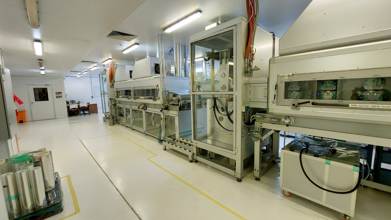
Implementation of the first large-format industrial printing line, marking a decisive step from laboratory-scale prototyping to industrial-scale manufacturing capability. This milestone completed the transition from Development [D] to early Innovation [I], with technology demonstrated in a relevant operational environment. Infrastructure included printing, encapsulation, assembly line, ink manufacturing, and accelerated testing & lifetime validation capabilities.
Market rollout for fullerene-based printed semiconductors targeting traditional silicon-based markets, completing the first full Lab-to-Fab-to-Market cycle. Technology was qualified in operational environments with pilot installations and application development programs. This phase validated the Innovation [I] pillar — implementing solutions in real market environments with a focus on cost reduction and scalability optimization.
Expansion of the Lab-to-Fab-to-Market rollout program into North America, with the establishment of a dedicated US operation under the brandname ORENgE®. Multiple pilot installations and commercial deployments were completed across key verticals — including BIPV, VIPV, and specialty applications — validating the technology under real-world conditions in the US market. This phase marked the transition from domestic operations to a truly international commercial footprint, building direct relationships with North American clients, suppliers, and institutional partners.
After a proven track record, CSEM Brasil adopted a new identity as ONINN, consolidating its Lab-to-Fab-to-Market platform and enabling greater flexibility in international partnerships. This transition marked a deliberate strategic decision to target R&D programs focused on high efficiency deposition materials based on NFA and PVK formulations for high performance energy devices.
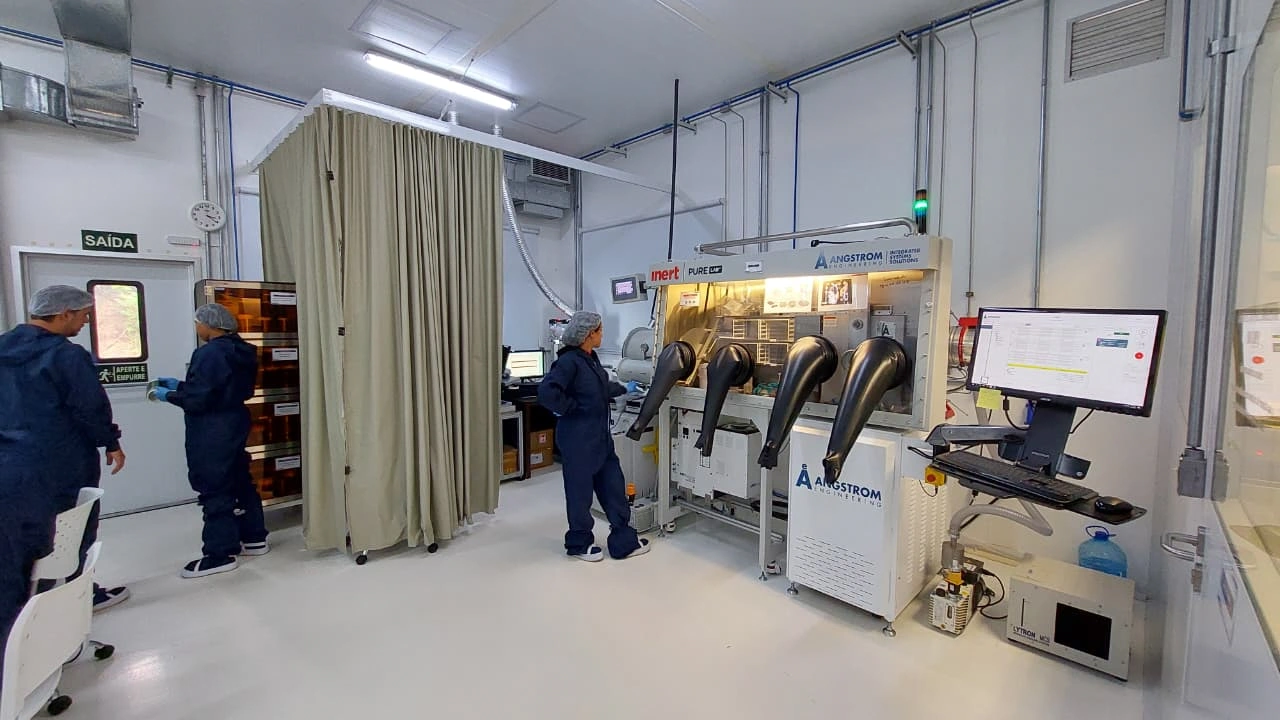
Major expansion of NFA and Perovskite (PVK) infrastructure for RD&I and scale-up, as part of an ongoing technology expansion program. New capabilities include dedicated NFA printing, PVK printing, and laser patterning equipment — initiating a new development cycle for next-generation materials while leveraging the existing manufacturing platform. This parallel development track enables the group to advance multiple semiconductor chemistries simultaneously through its established Lab-to-Fab-to-Market pipeline.
Completion of the Strategic Defense Certification Program, achieving the designation of Empresa Estratégica de Defesa (EED) — a formal accreditation granted by Brazil's Ministry of Defense recognizing PHD Semicon as a strategic defense company. This qualification enables PHD Semicon to participate in strategic defense procurement programs, access dedicated defense R&D funding mechanisms, and develop Man-Portable Solar Power (M-PSP) systems and other military-grade energy harvesting solutions for multiple armed forces and defense markets.
ONINN was incorporated as part of the group PHD Semicon, consolidating all operations under a single, focused mission: the development of printed semiconductor technologies on flexible polymeric substrates for energy generation and storage. The full vertical integration of the group — from laboratory research through industrial fabrication to targeted market deployment — positions PHD Semicon as a uniquely capable platform in the printed electronics landscape, with ongoing consolidation of its Lab-to-Fab-to-Market platform by expanding its ecosystem of partnerships and RD&I capabilities.
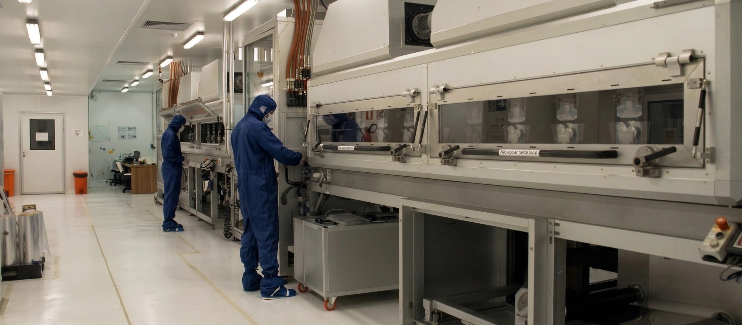
PHD Semicon is focused on mastering printed semiconductor technology within targeted, high-value applications — building the deep technical credibility and industrial capability that will define our platform for the future.
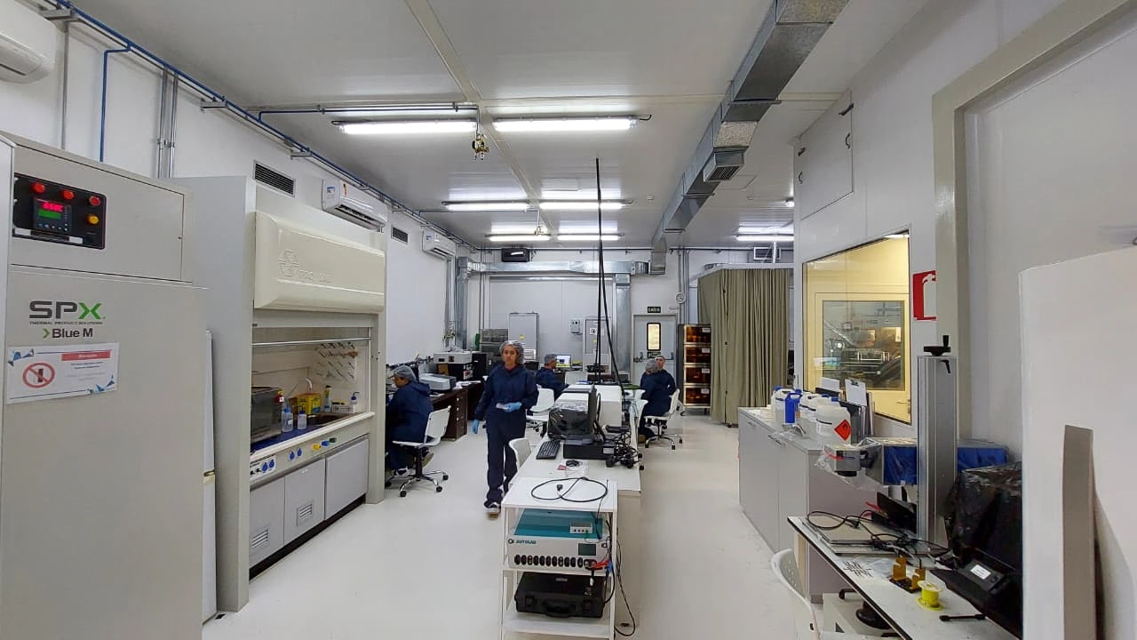
Our TechnologyPHD Semicon operates through a structured Research, Development & Innovation framework by operating its own private technology institute (ICT) — ensuring every technology we advance is grounded in scientific rigor and validated at each stage before progressing.
Fundamental scientific research validating chemical and physical concepts, confirming future applicability in energy generation and storage markets. Science-based investigation of new materials, device architectures, and printing processes.
Technological development translating validated research into scalable, performance-proven solutions in controlled industrial environments. Bridging laboratory concepts and manufacturing reality.
Applied innovation deploying mature technologies in real market environments — with a focus on cost optimization, scalability, and continuous performance improvement based on field data.
Our international network spans research institutions, industry partners, and government agencies across multiple continents.